 Out4Mind Your multi-thematic blog
Logic Gates
More articles under development…
Gate symbols
Having met the Boolean operations in the previous articles, let’s now take a look in the most common symbols used to represent our logic operators. The following symbols actually represent a logic circuit, though we call them logic gates.

AND

OR

XOR

NOT
Sometimes we need to have the outputs of these ports inverted, so we need to perform a NOT operation on their output. We saw this, for instance, in the Laws of De Morgan, where we find the results of an AND or OR operation inverted. So we could just use a AND gate, OR gate or XOR gate and connect a NOT gate ahead. However, we already have gates that perform this operation for us, by returning the negation of an AND, OR or XOR. They are represented by the following symbols:

NAND

NOR

NXOR
The truth tables for these operators are very easy and straight forward:
| NAND | 0 | 1 |
|---|---|---|
| 0 | 1 | 1 |
| 1 | 1 | 0 |
| NOR | 0 | 1 |
|---|---|---|
| 0 | 1 | 0 |
| 1 | 0 | 0 |
| NXOR | 0 | 1 |
|---|---|---|
| 0 | 1 | 0 |
| 1 | 0 | 1 |
It’s also common to have to invert one or more inputs we want to connect to our gates. In this case we will always need to use a NOT gate to invert that inputs before connecting them to the desired gates. However, when drawing a logic diagram, we can replace the NOT symbol with just a circle in the input of the gate. The following figures show that equivalence.
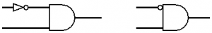
But let me remind you that, in this case, it’s really just a way to simplify the design. When we finally build the circuit itself, we need to use a NOT gate to invert that input.
Common logic families
When we start talking about logic gates we should keep in mind that there are several chips that allow us to build our logic circuit. By using defined voltages at their inputs we can represent a logic “0” or a logic “1”. In the beginning of the computer era, many computers were still using vacuum tube circuits, but soon the first transistors started to emerge and with them one of the first families of logic circuits such as the DTL (Diode-Transistor Logic). As the semiconductors kept evolving, a logic family has stood out and still today has its place in the market, the TTL (Transistor-Transistor Logic) family, also known by its 74xx chip series. However, in present days, technology is allowing us to build very tiny transistors, working at lower voltages and consuming less power, bringing up to us the CMOS (Complementary metal–oxide–semiconductor) technology, which is present in the smashing majority of computer and mobile devices.
As an example, let’s take a look at some of the 74xx chips from the TTL’s family:
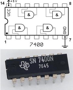
Internal diagram of a 7400 (quad 2-input NAND) and the chip itself. Source:: WikiCommon
- 7400 : Quad 2-iput NAND
- 7402: Quad 2-input NOR
- 7404: Hex NOT (6 inverters)
- 7408: Quad 2-input AND
- 7410: Triple 3-input NAND
- 7420: Dual 4-input NAND
- 7428: Quad 2-input NOR
- …
In the figure at the right, we have a 7400, a quad 2-input NAND gate. At the top we can see it’s diagram showing the internal connections of its four NAND gates throughout its 14 pins and, at the bottom, a photo of the chip itself. If we take a look at the diagram, we can see that pins 7 and 14 are used to power the chip with 5V (VCC – continuous current) in pin 14 and 0V (ground, black terminal in the power source) in pin 7. With this chip we can use up to 4 NAND gates with 2 inputs. For instance, in our logic functions we saw we have our input variables, so imagine we need to perform a NAND operation with 2 input variables. To do so, we can connect one of the variable to the pin 1 and the other variable to the pin 2. At pin 3, the output, we will get the result.
As we already mentioned, the value of a bit is represented by a determined voltage value. For example, in a typical TTL circuit, a bit with a “zero” is represented by a voltage of 0V and a bit with a “one” is represented by a voltage of 5V. So, for instance, if we connect both pins 1 and 2 of a 7400 to the ground (0V) we will get 5V in pin 3 (the output), because “0 NAND 0 = 1”
There are many variants of the TTL family where we can find different operating voltages, response speeds, and so on. I’m not going to enter on such details here, so if you’d like to read more about it, I recommend you the following Wikipedia’s article: 7400 series
From the logic function to the logic circuit
We saw we can create logic functions to address specific solutions, like activating the motor of a lift. And that is just a very small example in millions of possible applications, if you think how many complex circuits you have on a plane, with sensors to get the altitude, speed, pitches, and outputs to engines, flaps, etc… And many of these circuits must act on something (output) according to their inputs. Indeed, we have a vast world of digital circuits but to build one we need to know the basis and how it all starts: With a logic function.
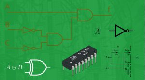
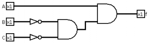
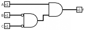
So, having a logic function that satisfies a determined solution, for a determined application, we can easily draw the equivalent circuits. To start with an easy example, let’s take the function we saw in the previous article:
f(a,b,c) = a . b . c
We can now draw the circuit using 2 NOT gates a 2 “2-input” AND gates:
Remember we can simplify the design by replacing the NOT gates by dots at the inputs of the AND gates, but remember also that you’ll always need the NOT gates:
And to have a nice picture of what were are dealing with here, we could draw an implementation of this circuit, using real TTL family chips, as follow:
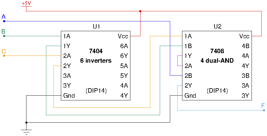
I’ve used colours in the lines just to help you to see the connections between our inputs, the chip’s pins and the output. When we use integrated circuits (chips) we use to name them U1, U2, … and it’s common to find, in the TTL chip’s pin out, a number and a letter. The number indicates the gate’s number, the letters A and B are for inputs and the letter Y is used for outputs. For instance, we know from the logic functions that we have to invert the inputs B and C, so they need to go through the inverter (7404). The input B enters in pin 1A and C in pin 2A, therefore we will have B in 1Y and C in 2Y. These last outputs will connect to the inputs 1A and 1B of the 7408 (AND) to perform the operation B AND C, having the result in 1Y connected to the input 2A. Finally, we connect the input variable A on 2B and we will have our function output F in pin 2Y.
Please remember that the AND operator is commutative, so in the 7408, the connections we made in 1A and 1B or in 2A and 2B can be switched. Also, what we want to do is to use NOT and AND gates available in the chips and it’s totally irrelevant the order of the gates we choose. It might even be useful to choose determined gates to make the connections easier, specially if we are designing a printed circuit board (PCB).
Soon we will be talk about Karnough maps and how to simplify locig functions. Follow us in the social networks and keep updated with our new posts!
References:
- Wikipedia: Boolean algebra
- Wikipedia: Logic family
Recommended software for designing logic circuits (Open Source):


